- 您现在的位置:买卖IC网 > Sheet目录1245 > SP720ABT (Littelfuse Inc)TVS ARRAY ESD 14 INPUT 16-SOIC
�� �
�
�TVS� Diode� Arrays�
�Electronic� Protection� Array� for� ESD� and� Overvoltage� Protection�
�SP720�
�Absolute� Maximum� Ratings�
�Continuous� Supply� Voltage,� (V+)� -� (V-).� .� .� .� .� .� .� .� .� .� .� .� .� .� .� .� .� .� .� .� .� .� .� .� .� +35V�
�Forward� Peak� Current,� IIN� to� VCC,� IIN� to� GND�
�(Refer� to� Figure� 6)� .� .� .� .� ..� .� .� .� .� .� .� .� .� .� .� .� .� .� .� .� .� .� .� .� .� .� .� .� .� .� .� .� .� ±2A,� 100μs�
�ESD� Ratings� and� Capability� (Figure� 1,� Table� 1)�
�Load� Dump� and� Reverse� Battery� (Note� 2)�
�Thermal� Information�
�Thermal� Resistance� (Typical,� Note� 1).� .� .� .� .� .� .� .� .� .� .� .� .� .� .� .� .� .� .� .� .� θ� JA� (� o� C/W)�
�PDIP� Package� .� .� .� .� .� .� .� .� .� .� .� .� .� .� .� .� .� .� .� .� .� .� .� .� .� .� .� .� .� .� .� .� .� .� .� .� .� .� .� .� .� .� .� .� .90�
�SOIC� Package� .� .� .� .� .� .� .� .� .� .� .� .� .� .� .� .� .� .� .� .� .� .� .� .� .� .� .� .� .� .� .� .� .� .� .� .� .� .� .� .� .� .� .� 130�
�Maximum� Storage� Temperature� Range� .� .� .� ..� .� .� .� .� .� .� .� .� .� .� .� .� .� .� -65� o� C� to� 150� o� C�
�Maximum� Junction� Temperature� (Plastic� Package)� .� .� .� .� .� .� .� .� .� .� .� .� .� .� .� .� .� .� .� .� .� 150� o� C�
�Maximum� Lead� Temperature� (Soldering� 10s)� .� .� .� .� .� .� .� .� ..� .� .� .� .� .� ..� .� .� .� .� .� .� .� .� .300� o� C�
�(SOIC� Lead� Tips� Only)�
�CAUTION:� Stresses� above� those� listed� in� “Absolute� Maximum� Ratings”� may� cause� permanent� damage� to� the� device.� This� is� a� stress� only� rating� and� operation� of� the� device�
�at� these� or� any� other� conditions� above� those� indicated� in� the� operational� sections� of� this� specification� is� not� implied.�
�NOTE:�
�1.� θ� JA� is� measured� with� the� component� mounted� on� an� evaluation� PC� board� in� free� air.�
�Electrical� Specifications� TA� =� -40� o� C� to� 105� o� C;� VIN� =� 0.5VCC� ,� Unless� Otherwise� Specified�
�PARAMETER�
�Operating� Voltage� Range,�
�SYMBOL�
�V� SUPPLY�
�TEST� CONDITIONS�
�MIN�
�-�
�TYP�
�2� to� 30�
�MAX�
�-�
�UNITS�
�V�
�V� SUPPLY� =� [(V+)� -� (V-)]�
�Forward� Voltage� Drop:�
�I� IN� =� 1A� (Peak� Pulse)�
�IN� to� V-�
�IN� to� V+�
�V� FWDL�
�V� FWDH�
�-�
�-�
�2�
�2�
�-�
�-�
�V�
�V�
�Input� Leakage� Current�
�Quiescent� Supply� Current�
�Equivalent� SCR� ON� Threshold�
�Equivalent� SCR� ON� Resistance�
�Input� Capacitance�
�Input� Switching� Speed�
�I� IN�
�I� QUIESCENT�
�C� IN�
�t� ON�
�Note� 3�
�V� FWD� /I� FWD� ;� Note� 3�
�-20�
�-�
�-�
�-�
�-�
�-�
�5�
�50�
�1.1�
�1�
�3�
�2�
�20�
�200�
�-�
�-�
�-�
�-�
�nA�
�nA�
�V�
�?�
�pF�
�ns�
�5�
�NOTES:�
�2.� In� automotive� and� battery� operated� systems,� the� power� supply� lines� should� be� externally� protected� for� load� dump� and� reverse� battery.� When� the�
�V+� and� V-� pins� are� connected� to� the� same� supply� voltage� source� as� the� device� or� control� line� under� protection,� a� current� limiting� resistor� should�
�be� connected� in� series� between� the� external� supply� and� the� SP720� supply� pins� to� limit� reverse� battery� current� to� within� the� rated� maximum�
�limits.� Bypass� capacitors� of� typically� 0.01� μ� F� or� larger� from� the� V+� and� V-� pins� to� ground� are� recommended.�
�3.� Refer� to� the� Figure� 3� graph� for� definitions� of� equivalent� “SCR� ON� Threshold”� and� “SCR� ON� Resistance.”� These� characteristics� are� given� here�
�for� thumb-rule� information� to� determine� peak� current� and� dissipation� under� EOS� conditions.�
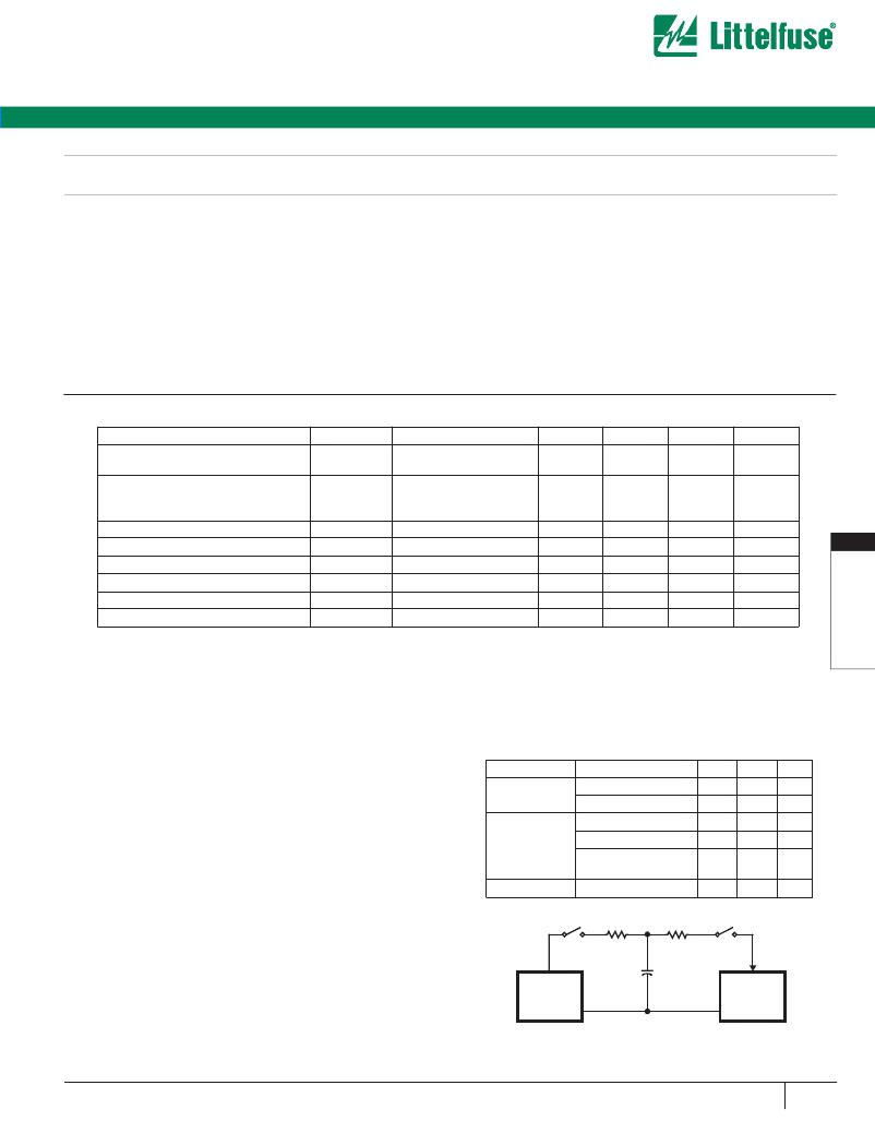
�ESD� Capability�
�TABLE� 1.� ESD� TEST� CONDITIONS�
�ESD� capability� is� dependent� on� the� application� and� defined� test�
�STANDARD�
�TYPE/MODE�
�R� D�
�C� D�
�±� V� D�
�standard.� The� evaluation� results� for� various� test� standards� and� methods�
�based� on� Figure� 1� are� shown� in� Table� 1.�
�MIL� STD� 3015.7� Modified� HBM�
�Standard� HBM�
�1.5k� ?� 100pF� 15kV�
�1.5k� ?� 100pF� 6kV�
�For� the� “Modified”� MIL-STD-3015.7� condition� that� is� defined� as� an�
�IEC� 61000-4-2�
�HBM,� Air� Discharge�
�330� ?� 150pF� 15kV�
�“in-circuit”� method� of� ESD� testing,� the� V+� and� V-� pins� have� a� return� path�
�to� ground� and� the� SP720� ESD� capability� is� typically� greater� than� 15kV�
�from� 100pF� through� 1.5k� ?� .� By� strict� definition� of� MIL-STD-3015.7� using�
�“pin-to-pin”� device� testing,� the� ESD� voltage� capability� is� greater� than� 6kV.�
�HBM,� Direct� Discharge�
�HBM,� Direct� Discharge,�
�Two� Parallel� Input� Pins�
�330� ?� 150pF�
�330� ?� 150pF�
�4kV�
�8kV�
�The� MIL-STD-3015.7� results� were� determined� from� AT&T� ESD� Test�
�EIAJ� IC121�
�Machine� Model�
�0k� ?�
�200pF�
�1kV�
�Lab� measurements.�
�The� HBM� capability� to� the� IEC� 61000-4-2� standard� is� greater� than� 15kV�
�for� air� discharge� (Level� 4)� and� greater� than� 4kV� for� direct� discharge�
�(Level� 2).� Dual� pin� capability� (2� adjacent� pins� in� parallel)� is� well� in� excess�
�CHARGE�
�SWITCH�
�R� 1�
�R� D�
�DISCHARGE�
�SWITCH�
�of� 8kV� (Level� 4).�
�For� ESD� testing� of� the� SP720� to� EIAJ� IC121� Machine� Model� (MM)� standard,�
�the� results� are� typically� better� than� 1kV� from� 200pF� with� no� series� resistance.�
�H.V.�
�SUPPLY�
�°±� V� D�
�C� D�
�IN�
�DUT�
�IEC� 1000-4-2:� R� 1� 50� to� 100M� ?�
�MIL� STD� 3015.7:� R� 1� 1� to� 10M� ?�
�FIGURE� 1.� ELECTROSTATIC� DISCHARGE� TEST�
�w� w� w.� l� i� t� t� e� l� f� u� s� e� .� c� o� m�
�229�
�发布紧急采购,3分钟左右您将得到回复。
相关PDF资料
SP721ABG
TVS ARRAY ESD 6 INPUT 8-SOIC
SP721ABT
TVS ARRAY ESD 6 INPUT 8-SOIC
SP723ABT
TVS ARRAY ESD 6 INPUT 8-SOIC
SP723APP
TVS ARRAY ESD 6 INPUT 8-DIP
SP724AHTG
TVS ARRAY ESD 4 INPUT SOT-23
SP724AHT
TVS ARRAY ESD 4 INPUT SOT-23
SPC02SVDN-RC
CONN JUMPER SHORTING .100" GOLD
SPC02SVGN-RC
CONN JUMPER SHORTING .100" GOLD
相关代理商/技术参数
SP720ABTG
功能描述:TVS二极管阵列 30V 1A 3pF 14 Input RoHS:否 制造商:Littelfuse 极性: 通道:4 Channels 击穿电压: 钳位电压:11.5 V 工作电压:2.5 V 峰值浪涌电流:20 A 安装风格:SMD/SMT 端接类型:SMD/SMT 系列: 最小工作温度:- 40 C 最大工作温度:+ 85 C
SP720ABTG
制造商:Littelfuse 功能描述:Diode 制造商:Littelfuse 功能描述:DIODE, TVS, 3pF, SOIC-16
SP720ABTG-CUT TAPE
制造商:LITTELFUSE 功能描述:SP720 Series 3 pF Surface Mount Electronic Protection Array for ESD - SOIC-16
SP720AP
功能描述:TVS二极管阵列 SP720AP RoHS:否 制造商:Littelfuse 极性: 通道:4 Channels 击穿电压: 钳位电压:11.5 V 工作电压:2.5 V 峰值浪涌电流:20 A 安装风格:SMD/SMT 端接类型:SMD/SMT 系列: 最小工作温度:- 40 C 最大工作温度:+ 85 C
SP720APP
功能描述:TVS二极管阵列 14 CH DIODE ARRAY RoHS:否 制造商:Littelfuse 极性: 通道:4 Channels 击穿电压: 钳位电压:11.5 V 工作电压:2.5 V 峰值浪涌电流:20 A 安装风格:SMD/SMT 端接类型:SMD/SMT 系列: 最小工作温度:- 40 C 最大工作温度:+ 85 C
SP720APP - LITTELFUSE
制造商:Littelfuse 功能描述:DIODE TVS 制造商:Littelfuse 功能描述:DIODE, TVS
SP720APP
制造商:Littelfuse 功能描述:TVS DIODE ARRAY
SP720APP
制造商:Littelfuse 功能描述:THYRISTOR ARRAY TVS